TSMC battles to stay ahead as world demands ever-smaller chips

Roula Khalaf, Editor of the FT, selects her favourite stories in this weekly newsletter.
Smartphone chip design house MediaTek had only praise for Taiwan Semiconductor Manufacturing Company in a presentation at the world’s largest contract chipmaker’s recent tech symposium. The success of MediaTek’s latest flagship processor “is rooted in the work our partners at TSMC have done together with us,” it said.
But TSMC chief executive CC Wei winced when the presentation showed that its further miniaturisation of the chip — to create circuits around 4 billionths of a metre wide — had only produced a 2 per cent increase in performance.
“When I saw [that], I almost fell off my chair,” Wei said.
Chipmakers are bumping up against the laws of physics as they strive to make semiconductors ever faster and more power-efficient, in order to enable rapidly evolving applications from high-end gaming on smartphones to servers being used for climate change simulation.
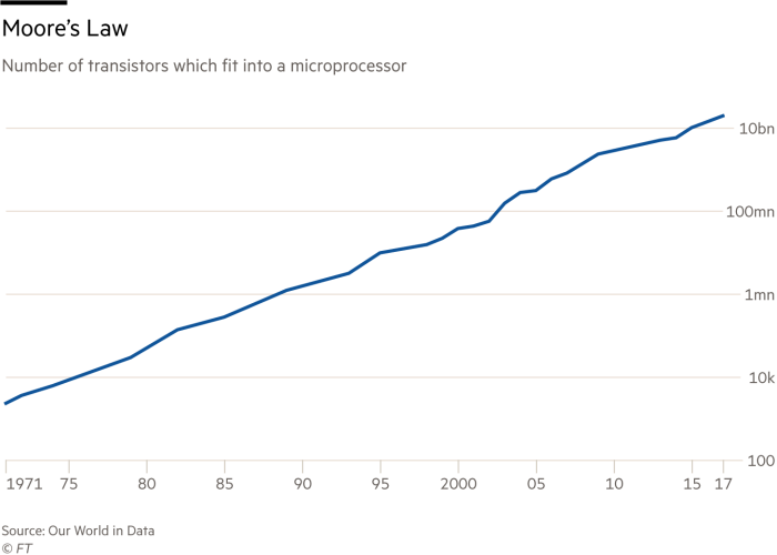
Seventy-five years after the invention of the transistor, a switch that controls electrical current and forms the heart of every semiconductor, the principle that the number of transistors packed on each chip will double around every two years, enabling explosive growth of computing power, is crumbling. Shrinking them is getting too difficult.
“Just relying on transistors is no longer enough to meet our demands today, and to meet [the requirements of] the products you design,” Wei told an audience of TSMC customers.
In 1965, Gordon Moore, co-founder of Fairchild Semiconductor and later Intel, had observed the doubling of the transistor count per chip around every 24 months and predicted such exponential growth for the next decade. So-called Moore’s Law held true much longer than its inventor had foreseen — one IC device can contain up to 100bn transistors today, according to TSMC — but it is now reaching a limit.

This challenge of finding technical alternatives is making competition among the world’s top chip manufacturers more unpredictable, although, for now, TSMC has a clear lead in manufacturing technology.
Its foundry business model of only manufacturing semiconductors to other companies’ designs has helped it capture more than half of the global market for made-to-order chips, with more than 12,000 different products made and close engineering relationships with over 500 customers.
Previously, Intel squandered its manufacturing lead over TSMC with a series of missteps in its last two process node transitions, and is now reckoned to be around two years behind. But analysts say that could change, especially as governments from the US to Japan are pushing chipmakers to localise production with big subsidies that could favour Intel and TSMC’s other main rival Samsung.
“[TSMC] could stumble. As moving to the next technology node becomes more difficult, anyone could stumble,” said Chris Miller, an economic historian at Tufts University who has written a book on the chip industry’s history. “Or, if the next couple of process technology node transitions are harder than we expect, TSMC’s edge could become less meaningful.”
Chipmakers have battled the slowdown of Moore’s Law successfully for more than a decade. When packing more transistors ran into problems, they started stacking them on top of each other. They are also packaging different chips together on one piece of silicon, rather than across a PC motherboard — TSMC uses such multi-die package technology to make the Epyc, AMD’s data centre processor.
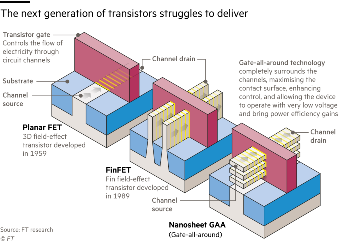
But now, the industry is being forced to look at other enhancements. As the so-called FinFET process used for the past decade can no longer deliver enough gains in speed and power, it is adopting a new transistor architecture.

Beginning from N2 — the generation of chips that TSMC plans to mass-produce from 2025 — it will use a technology it calls Nanosheet and which is also known as Gate-All-Around (GAA).
Under that architecture, the transistor gate, which controls the flow of electricity through circuit channels, completely surrounds the channels rather than being on three sides, as in the previous solution. This maximises the surface and “allows the device to operate with very low voltage and bring power efficiency gains,” said Kevin Zhang, vice-president at TSMC.
The transition is proving difficult though. Samsung, which tried to pioneer GAA at the N3 generation, has struggled to raise its yield — the proportion of non-defective chips that are produced. It started mass production in June at N3 — just before TSMC, which is to start volume production before the end of the year.
Samsung’s yield problem is making it struggle to attract big customers for the cutting-edge chip production. Analysts do not expect its earlier adoption of GAA to help it catch up with TSMC anytime soon, but said it could attract big customers like Google and Tesla once it introduces a second-generation GAA N3 process next year and secures a stable yield.
TSMC executives indicated that their decision to stick with the previous architecture at N3 is paying off. “It allowed us to bring N3 to the market faster,” Zhang said. The company said it is achieving “good yields”, and customer demand for N3 is so strong that it is putting a strain on its engineering capacity. TSMC has commitments from Apple, Intel, AMD and several other customers for N3.
Meanwhile, Intel has laid out an ambitious goal of matching TSMC’s process technology by 2024 and overtaking it a year later — though the continuing slide in its stock price shows that Wall Street is not yet convinced it can both fix its previous missteps and catch up with TSMC's headlong technology advances by then. The US chipmaker plans to make a belated switch to the most advanced EUV manufacturing equipment next year and adopt its own version of GAA in 2024, to produce a chip with features 2nm wide.
But as much as TSMC is confident in its leading position now, even larger challenges loom in the future. Chipmakers expect that key tools and materials used for making semiconductors for decades will need to be significantly changed or even replaced before long, and eventually the days of silicon itself, the base material of the industry since its inception, will be numbered.

Comments